
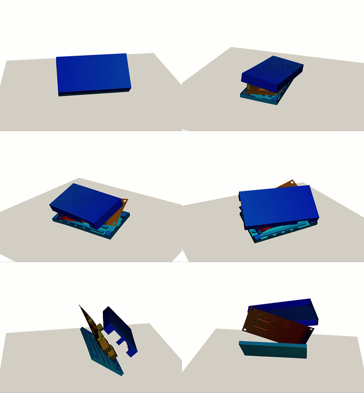
Designing a durable electronic enclosure is one of the most critical stages in bringing a physical hardware product to market. For both established companies and agile startups, a single accidental drop can shatter a product’s casing, dislodge internal components, or break delicate solder joints, leading to costly failures. Historically, avoiding these disasters required building numerous physical prototypes and dropping them in a lab until they broke. Today, integrating Finite Element Analysis (FEA) simulation directly into the design workflow transforms this chaotic, expensive process into a streamlined, highly predictable business operation.
Eliminating the Costly Prototype Loop
In traditional product development, engineers design a casing, wait weeks for a prototype to be manufactured, and then physically drop it to see where it cracks. If it fails, the design goes back to the drawing board, and the expensive prototyping cycle repeats. FEA simulation completely disrupts this loop by creating a virtual drop test environment. Engineers can subject a digital 3D model of the enclosure to various drop heights, impact angles, and floor surfaces before a single physical part is ever made. This drastically cuts down on material waste, tooling modifications, and manufacturing costs, allowing startups to conserve precious capital and larger firms to optimize their development budgets.
Accelerating Time-to-Market
In competitive technology markets, being first to market can define a company’s success. Relying solely on physical testing introduces massive scheduling bottlenecks, especially if long lead times are required for injected-molded plastics or CNC-machined parts. By utilizing FEA drop tests, design flaws such as high-stress concentrations, weak snap-fits, or inadequate rib reinforcements are identified in hours rather than weeks. Companies can iterate through dozens of design variations in a fraction of the time, confidently locking in a optimized design and significantly compressing the product launch timeline.
Optimizing Material Selection and Weight
When designing a handheld or portable electronic device, finding the perfect balance between structural strength and minimal weight is a constant challenge. FEA simulation allows engineering teams to virtually experiment with various polymers, composites, or lightweight alloys. The software provides detailed visual stress heatmaps, pinpointing exactly where the enclosure needs thicker walls and where material can be safely stripped away. This optimization process prevents over-engineering, reduces final manufacturing part weight, and lowers shipping costs, directly improving the product’s gross margins.
Protecting Internal Components and Reliability
An electronic enclosure does more than just look good; its primary job is to shield the sensitive electronics inside from impact energy. When a device hits the ground, a severe shockwave travels through the casing and into the printed circuit board (PCB), batteries, and connectors. FEA drop testing simulates this internal energy transfer, allowing engineers to measure the G-forces experienced by fragile components. By visualizing how the shock wave propagates, teams can design better internal shock-absorbing mounts, place dampening materials strategically, and prevent catastrophic internal component failure, ensuring a highly reliable product.
Boosting Investor Confidence and Brand Reputation
For startups seeking venture capital or companies launching a new product line, demonstrating technical maturity is essential. Presenting rigorous FEA simulation data and drop test reports to investors or stakeholders proves that the product is engineered to last, reducing perceived technical risks. Furthermore, launching a product that survives real-world drops builds immense customer trust and protects the brand from the devastating financial and reputational impacts of mass product recalls, negative online reviews, and excessive warranty claims.
Author: Caesar Wiratama
Find me on Linkedin